Special thanks to: Bob VanderClay, Ben Hanor, Alberto Covarrubias and Amos Bieler for contributing info to this document.
Notes and Disclaimer: All data within this manual was collected from public domain sources or through reverse engineering. All information is provided as is, there is no warranty either real or implied with this information, use at your own risk.
Virtual Boy, Nintendo, and Game Boy are registered trademarks of Nintendo CO., LTD.
v810, and NEC are registered trademarks of NEC Corp.
All rights are held by their respective companies.
This document and all information within copyright © 1999-2000 David Tucker and Amos Bieler.
1. Introduction
The Virtual Boy (VB) is a portable, stereoscopic, videogame device developed by Gunpei Yokoi (1941-1997) for Nintendo. It features a red LED-based 384x224 four 'color' display for each eye and a ca. 20MHz NEC v810 RISC CPU.
Originally released in 1995 for around $200 in the US, the VB quickly fell under intense criticism from the video game industry for being over priced and unimpressive. Nintendo let the system flounder for only a year before pulling the plug on it, making it the only system released by Nintendo to date that was a major flop. When the dust had settled, there where 14 titles released in both the US and Japan, plus 8 titles released only in Japan.
How to Read This Document
To understand the internals and code that follows, you will need at least a rudimentary understanding of assembly language and the inner workings of a computer (memory, CPU, I/O, etc.)
In this document, I assume that you understand the difference between Decimal, Binary and Hex number systems, (Base-10, Base-2 and Base-16, respectively) and how to convert between them.
2. Requirements
Here is a list of VB related things you can do, and what you need to do them:
3. Hardware Overview
The VB hardware consists of:
4. Hardware Detail
Video Overview
Graphics on the VB are defined using Chars, BGMaps, OBJs, and Worlds.
A Char is an individual 8x8 pixel, four color bitmap, and is the basic element upon which all VB graphics are based. Both BGMaps and OBJs are collections of Chars.
BGMaps are like checker boards made of 64x64 Chars (512x512 pixels.) Since one can 'move' the whole BGMap relative to it's World, but not move the individual Chars relative to each other, they are best at displaying large scenes like background graphics.
OBJ collections are like BGMaps, in that they are groups of individual Chars. However, the Chars in an OBJ collection - called, simply, OBJs - are separate and can be placed on pixel boundaries. There are a maximum of four such OBJ collections, each containing none, some or all of the 1024 (0x400) definable OBJs.
Worlds are like containers that hold BGMaps and OBJ collections. There are 32 Worlds, each containing either a BGMap-like collection of BGMaps (explained later) or one of the OBJ collections.
Worlds are drawn on top of one another so that non-transparent parts of closer Worlds cover up Worlds farther away. This helps create a 3D effect. The parallax values of each BGMap or OBJ, combined with that stored in each World, is used to generate a different image for each of the VB's two displays.
These different images, displayed to each of the user's eyes, are what produce the stereoscopic 3D effect. There are two ways to do this with the internal sprite engine:
The easiest (and, thus, more common) method requires only a single image for each Char, shared between the two displays. To achive a stereoscopic effect, it has a different horizontal position for each eye, using the parallax attribute. Positive values for parallax push the image further away from you and negative values bring it closer.
| Pros | Cons |
|---|---|
| * Only one OBJ required per 'character' * Takes up less room in ROM * Easier on art department ;^) | * 'Cardboard cut-out' effect isn't as realistic |
The other method involves creating a separate image for each display. This creates 3D objects, instead of 'cardboard cut-outs' that are simply on different 'planes.' Of course, when using this method, you can (and, most likely, will) use the parallax method, as well.
| Pros | Cons |
|---|---|
| * Richer, more realistic graphics | * Takes more room in ROM * Basically halves available Chars, OBJs etc. * Code is more complex |
The discussion thus far has assumed the use of the VB's sprite engine for graphics. While these methods apply to almost any imaginable game, some games require direct access to the screen buffers. This is possible on the VB, but it involves some additional timing which isn't fully understood at this time. Stay tuned...
Video Detail
Chars
Chars have the following characteristics:
Each Char requires 16 bytes and is stored in a non-interlaced, uncompressed form:
Char RAM contains 2048 (0x800) Chars, arranged into four segments in the VB's address space:
| Address Range | Chars | |
| 0x0000 6000 - 0x0000 7FFF | 0 - 511 (0x000 - 0x1FF) | |
| 0x0000 E000 - 0x0000 FFFF | 512 - 1023 (0x200 - 0x3FF) | |
| 0x0001 6000 - 0x0001 7FFF | 1024 - 1535 (0x400 - 0x5FF) | |
| 0x0001 E000 - 0x0001 FFFF | 1536 - 2047 (0x600 - 0x7FF) |
Char RAM is also mirrored into the range: 0x0007 8000 - 0x0007 FFFF, allowing linear access to all 2048 (0x800) Chars at once.
To access a given Char in Char RAM:
char[n] = n * 16 + 0x00078000
BGMaps
BGMaps are the static images on the VB Screen. BGMaps are composed of Cells, each cell containing a single Char. One BGMap is known as a segment. Each segment, a 64x64 (4096) Char (512x512 pixel) image, requires:
2 (bytes/cell) * 4096 (cells/segment) = 8192 bytes
And are laid out left to right, top to bottom:
| Row | |||||||
|---|---|---|---|---|---|---|---|
| 0 | 0 | 1 | 2 | ... | 61 | 62 | 63 |
| 1 | 64 | 65 | 66 | ... | 125 | 126 | 127 |
| . . . | |||||||
| 62 | 4016 | 4017 | 4018 | ... | 4029 | 4030 | 4031 |
| 63 | 4032 | 4033 | 4034 | ... | 4045 | 4046 | 4047 |
A maximum of 14 such segments may be stored in BAM (BGMap Attribute Memory), which starts at 0x0002 0000. It's upper bound (0x0003 C000 maximum) is variable, and is shared with the PARAM_TABLE, based on the number of active segments.
| F | E | D | C | B | A | 9 | 8 | 7 | 6 | 5 | 4 | 3 | 2 | 1 | 0 |
|---|---|---|---|---|---|---|---|---|---|---|---|---|---|---|---|
| BPLT | HFLP | VFLP | 0 | BCA (0 - 2047) | |||||||||||
|
OBJs
OBJs are used to represent small 'movable' objects, such as a game's protagonist.
OBJs are stored in OAM (OBJ Attribute Memory) which occupies the 8192 (0x02000) bytes from 0x0003 E000 to 0x0003 FFFF. Since each OBJ uses four HWords, (8 bytes) there is a total of 1024 (0x400) possible OBJs.
There are four offset registers in the VIP region (SPT0-SPT3) that break up OAM into four collections. A World may contain only one of these four OBJ collections.
When the graphics engine needs to draw a collection of OBJs, the display renderer starts at an SPT pointer (SPT3 is first) and counts backwards, drawing each OBJ where it goes. When it reaches the next lower SPT pointer, (actually, right before it...) it stops drawing.
An example:
    SPT3 = 0x300
    SPT2 = 0x200

    The first World containing an OBJ collection is encountered.

    OBJs 0x300 to 0x201 are displayed in that order:

        Address of first OBJ:
            OBJ Base Address (0x0003 E000) + SPT3 (0x300) = 0x0003 E300

        Start here and count back to...
            OBJ Base Address (0x0003 E000) + SPT2 (0x200) = 0x0003 E200

        ...drawing objects as we go.
OBJs differ from BGMaps in many ways:
This is great if you want to place a few Chars randomly about the screen, i.e. making bubbles or stars.
OBJ Attributes
| F | E | D | C | B | A | 9 | 8 | 7 | 6 | 5 | 4 | 3 | 2 | 1 | 0 |
|---|---|---|---|---|---|---|---|---|---|---|---|---|---|---|---|
| JX: -7 (-0x007) to 383 (0x17F) | |||||||||||||||
| JLON | JRON | JP: -256 (-0x100) to 255 (0x0FF) | |||||||||||||
| JY: -7 (-0x007) to 223 (0x0DF) | |||||||||||||||
| JPLT | HFLP | VFLP | 0 | JCA: 0 (0x000) to 2047 (0x7FF) | |||||||||||
|
Worlds
Worlds are collections of OBJs and BGMaps that are layered and clipped to fit each screen (384x224).
There are a total of 32 Worlds, but not all 32 Worlds need be used.
Worlds are drawn back to front, starting at 31 and ending with 0. Only Worlds with at least one visible bit set (LON || RON == 1) are drawn. If, however, a World is marked as the END World, it and all remaining Worlds are skipped.
As the VB renders the left and right screens, parallax is factored in, by subtracting GP from GX for the left screen, and adding GP to GX for the right screen. Any special effects, like sprite scaling, and rotation, are also rendered at this time.
32 Worlds x 16 HWords/World = 1024 (0x400) bytes.
World RAM is at 0x0003 D800 - 0x0003 DBFF
| F | E | D | C | B | A | 9 | 8 | 7 | 6 | 5 | 4 | 3 | 2 | 1 | 0 |
|---|---|---|---|---|---|---|---|---|---|---|---|---|---|---|---|
| LON | RON | BGM | SCX | SCY | OVR | END | 0 | 0 | BGMAP_BASE: 0 (0x0) to 13 (0xD) | ||||||
| GX (0x000 - 0x17F) | |||||||||||||||
| GP (-0x100 - 0x0FF) | |||||||||||||||
| GY (0x000 - 0x0DF) | |||||||||||||||
| MX (0x000 - 0xFFF) | |||||||||||||||
| MP (-0x100 - 0x0FF) | |||||||||||||||
| MY (0x000 - 0xFFF) | |||||||||||||||
| W (0x000 - 0xFFF) | |||||||||||||||
| H (0x000 - 0xFFF) | |||||||||||||||
| PARAM_BASE (0x0000 - 0xEBF0) *(see text) | |||||||||||||||
| OVERPLANE_CHARACTER | |||||||||||||||
| WRITING FORBIDDEN | |||||||||||||||
| WRITING FORBIDDEN | |||||||||||||||
| WRITING FORBIDDEN | |||||||||||||||
| WRITING FORBIDDEN | |||||||||||||||
| WRITING FORBIDDEN | |||||||||||||||
BGM Types
Normal: Cut an image from the BGMap(s) located at (MX - MP, MY) for the left eye and (MX + MP, MY) for the right eye, that are each W wide and H high. Paste these images at (GX - GP, GY) on the left screen and (GX + GP, GY) on the right screen.
The first BGMap is computed by taking the offset to BGMap memory (0x0002 0000) and adding BGMAP_BASE * 0x2000 (the size of one BGMap). Starting with this first BGMap and tile 2SCX BGMaps wide and 2SCY BGMaps high, using no more than eight BGMaps.
H-bias: This form is used for 'wavy' effects. Each row on the screen can be shifted by a factor left or right, and this shifting is separate for the left and right displays.
PARAM_BASE points to the base offset of the H-Bias parameter table. This table has a column for each display, each containing one HWord (16-bit) for each line to be displayed. For the whole screen, (384x224 pixels) the table would be...
	16 (bits/HWord) x 224 (rows/screen) x 2 (screens) =
	7168 bits / 8 (bits/byte) = 896 bytes
...in size.
When displaying this World, follow the procedures above to generate the data. But, when copying to the display buffer, modify the MX value by adding the current H-Bias table entry (-511 to 512) to it. Remember to use the appropriate value (H-biasL, or H-biasR) depending on the screen being rendered. So, to find the true MX value for each line of each screen, use:
	MXL = MX - MP + H-biasL
	MXR = MX + MP + H-biasR
Affine: This is used to display zooming and rotation effects. MX, MY, and MP are ignored in this mode, cut from the BGMap at (0, 0) [I think]. GX, GY, GP, X, and Y are all used just like the Normal mode. [MUCH more info needed!]
OBJ: Displays one of the four OBJ collections. OBJ collections are discussed above. OBJ groups ignore MX and MY, and possibly GX and GY, as well. The position of each OBJ in a collection is relative to screen coordinates (0, 0).
Brightness
The registers BRTA, BRTB, and BRTC are the three brightness registers. Each register holds an integer from 0 to 80 that defines the hardware brightness level for that color entry. BRTA and BRTB directly define their respective brightnesses. However, the true brightness of a palette color pointing to BRTC is:
BRTCT = BRTA + BRTB + BRTC
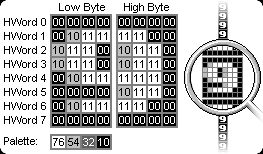
Palettes/Transparency
To allow for special palette tricks, such as the simulation of a lightning flash, the pixels of a char, rather than specifying a brightness directly, point to a 'color' in a 'palette.' A palette is an 8-bit number, composed of four 2-bit colors. The two least significant bits of a palette constitute color 0, bits 2 and 3 are color 1 etc.
There are four possible palettes for OBJs (JPLT0-JPLT4) and another four for BGMaps (GPLT0-GPLT4.)
BKCOL
The BKCOL register tells the system what color to clear the background to, before drawing the screen. The following values may be used:
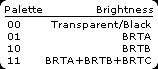
	0	Black
	1	BRTA
	2	BRTB
	3	BRTA + BRTB + BRTC
Repeat
[On by default? FRMCYC High Byte?]
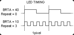
Since the VB uses scanning mirrors to generate the display, the dots aren't fixed in width. Instead, they vary in width based on their intensity. To help smooth out the dots and limit the gap between, the VB has a 'repeat' register [where?] that allows a given dot to turn on multiple times within a given dot period. Repeat takes the literal brightness (BRTA, BRTB and BRTC) of a given dot and repeats it the specified number of times, thus intensifying the dot by that number.
It is possible to change the repeat register once every display cycle, and also once every four columns of the display. By changing every four columns, you can give the illusion of having more colors active at a time.
For an example of using Repeat, imagine that you were setting up the BRTA register to an intensity of 40 (with Repeat set to the default 0). If you wanted to smooth out the appearance of the dot, you could set the Repeat value to three (repeat four times), and the BRTA register to 10, to achieve a smoother dot with an equivalent intensity.
Column Table
;----------------------------------------------------------------
lb. ColTblData
db. 0xfe, 0xfe, 0xfe, 0xfe, 0xfe, 0xfe, 0xfe, 0xfe
db. 0xfe, 0xfe, 0xfe, 0xfe, 0xfe, 0xfe, 0xfe, 0xfe
db. 0xfe, 0xfe, 0xfe, 0xfe, 0xfe, 0xfe, 0xfe, 0xfe
db. 0xfe, 0xfe, 0xfe, 0xfe, 0xfe, 0xfe, 0xfe, 0xfe
db. 0xfe, 0xfe, 0xfe, 0xfe, 0xfe, 0xfe, 0xfe, 0xfe
db. 0xfe, 0xfe, 0xfe, 0xfe, 0xfe, 0xfe, 0xfe, 0xfe
db. 0xfe, 0xfe, 0xfe, 0xfe, 0xfe, 0xfe, 0xfe, 0xfe
db. 0xfe, 0xfe, 0xfe, 0xfe, 0xfe, 0xfe, 0xe0, 0xbc
db. 0xa6, 0x96, 0x8a, 0x82, 0x7a, 0x74, 0x6e, 0x6a
db. 0x66, 0x62, 0x60, 0x5c, 0x5a, 0x58, 0x56, 0x54
db. 0x52, 0x50, 0x50, 0x4e, 0x4c, 0x4c, 0x4a, 0x4a
db. 0x48, 0x48, 0x46, 0x46, 0x46, 0x44, 0x44, 0x44
db. 0x42, 0x42, 0x42, 0x40, 0x40, 0x40, 0x40, 0x40
db. 0x3e, 0x3e, 0x3e, 0x3e, 0x3e, 0x3e, 0x3e, 0x3c
db. 0x3c, 0x3c, 0x3c, 0x3c, 0x3c, 0x3c, 0x3c, 0x3c
db. 0x3c, 0x3c, 0x3c, 0x3c, 0x3c, 0x3c, 0x3c, 0x3c
;----------------------------------------------------------------

lb. LoadColTblStart				;Write 1st 1/2 of ColTbl
	movhi		0x0004, $0, $3		;0x0003DC00 => $3
	movea		0xDC00, $3, $3		;Start of column table
	movhi		0x0004, $0, $4		;0x0003DCFF => $3
	movea		0xDCFF, $4, $4		;End of column table
	.mov32		ColTblData, $6		;Column Table data
lb. CTBL_Loop1
	ld.b		0x00[$6], $5		;Data to write
	shl		0x18, $5		;zero high bits
	shr		0x18, $5
	st.h		$5, 0x0000[$3]		;Column Table 1
	st.h		$5, 0x0200[$3]		;Column Table 2
	add		0x02, $3
	add		0x01, $6
	cmp		$4,$3
	bge		0x0C
	.jump		CTBL_Loop1
						;Write 2nd 1/2 of ColTbl
	movhi		0x0004, $0, $3		;0x0003DDC00 => $3
	movea		0xDD00, $3, $3		;Start of column table
	movhi		0x0004, $0, $4		;0x0003DDCFF => $3
	movea		0xDDFF, $4, $4		;End of column table
	.mov32		ColTblData, $6		;Column Table data
	addi		0x7F,$6,$6
lb. CTBL_Loop2
	ld.b		0x00[$6], $5		;Data to write
	shl		0x18, $5
	shr		0x18, $5
	st.h		$5, 0x0000[$3]		;Column Table 1
	st.h		$5, 0x0200[$3]		;Column Table 2
	add		0x02, $3
	add		-1, $6			;subtract 1
	cmp		$4,$3
	bge		0x0C
	.jump 		CTBL_Loop2
GClock
[Fill in later]
[FRMCYC Low Byte]
Physical Display
[Fill in later]
Direct Screen Buffer Access
[Fill in later]
Miscellaneous
Controller
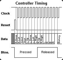
The procedure for a hardware Keypad read is:
;HCREG offset defines for readability
df. HCREGR_KLB	0x00000010
df. HCREGR_KHB	0x00000014
df. HCREGR_KCR	0x00000028

; Read Keypad, and store the 16-bit result in Register $3
					;Pointer to HCREG base:
movhi		0x0200, $0, $4		;$4 <= 0x02000000
movea		0x0080, $0, $2		;0x00000080 => $2
st.b		$2, HCREGR_KCR[$4]	;Tell Controller to reset
add		0x04, $2		;0x00000084 => $2
st.b		$2, HCREGR_KCR[$4]	;Tell Controller to read
ld.b		HCREGR_KCR[$4], $2	;Read status
andi		0x0002, $2, $2
bne		-8			;Keep reading until Zero
ld.b		HCREGR_KHB[$4], $2	;Read Upper Byte
shl		0x18, $2		;remove sign bit
shr		0x10, $2		;and shift left 8 bits
ld.b		HCREGR_KLB[$4], $3	;Read Lower Byte
shl		0x18, $3		;remove sign bit
shr		0x18, $3
or		$2, $3			;put them together in $3
Button Data
| F | E | D | C | B | A | 9 | 8 | 7 | 6 | 5 | 4 | 3 | 2 | 1 | 0 |
|---|---|---|---|---|---|---|---|---|---|---|---|---|---|---|---|
| rdd | rdl | sel | str | ldu | ldd | ldl | ldr | rdr | rdu | lbb | rbb | b | a | 1 | bat |
Link Port
(Fill in later)
Timer
(Fill in later)
Interrupts/timing
(Fill in later)
Sound
There are 6 sound sources in the VB, each source can be individually played on the left or right speaker, or both. Sounds 1-4 are standard voluntary wave pattern sounds, where the pattern generated for each sound is user definable in a 32x6-bit wave table. Sound 5 is a Sweep/Modulation sound source with separate wave tables for both. And sound 6 is a white noise source. Sound is sampled at 41.7Khz with a 13bit precision. Little is known at this time about the details.
Rest
(Fill in later)
Initialization
(Fill in later)
5. Memory Maps
Condensed Memory Map
The Virtual Boy uses 128 Mbytes of the 32bit CPU's 4 GB addressable area. A26 ~ A24 are decoded and the 128Mbyte area is divided into 8 16-Mbyte areas. So internally all memory addresses are masked with 0x07FF FFFF. Only the significant bits of each memory area are decoded, so memory 'mirrors' itself within these regions.
| VIP Area: control registers, VRAM, DRAM | 0x00000000 - 0x0007FFFF |
| IMAGE | 0x00080000 - 0x00FFFFFF |
| Sound Area: control registers, data | 0x01000000 - 0x01FFFFFF |
| Hardware Control Area: Wait States, Key Pad, Link Port, Timer | 0x02000000 - 0x020000xx |
| IMAGE | 0x020000xx - 0x02FFFFFF |
| UNUSED | 0x03000000 - 0x03FFFFFF |
| Game Pak Expansion Area: SuperF/X chips 'n' stuff | 0x04000000 - 0x04FFFFFF |
| NVC WRAM AREA: 64Kbytes | 0x05000000 - 0x0500FFFF |
| IMAGE | 0x05010000 - 0x05FFFFFF |
| Game Pak RAM area: 16Mbytes max | 0x06000000 - 0x06FFFFFF |
| Game Pak ROM area: 16Mbytes max | 0x07000000 - 0x07FFFFFF |
Detailed Memory Map
Located in this separate file.
ROM 'Header' Info
The game header info, actually at the end of the ROM, is mapped down from 0x07FF FFFF. Since the ROM replicates itself from 0x0700 0000 to 0x07FF xxxx, and we mask off the higher address lines, 0x07FF FFFF is always at the end of the ROM, no matter the size.
| 0x07FF FDE0 - 0x07FF FDF3 | Game Title |
| 0x07FF FDF4 - 0x07FF FDF8 | Reserved |
| 0x07FF FDF9 - 0x07FF FDFA | Manufacturer |
| 0x07FF FDFB - 0x07FF FDFE | Game ID |
| 0x07FF FDFF | ROM Version (1.x) |
Interrupt Vectors
0xFFFF FE00 - 0xFFFF FE0F   INTKEY	Controller Interrupt
0xFFFF FE10 - 0xFFFF FE1F   INTTIM	Timer Interrupt
0xFFFF FE20 - 0xFFFF FE2F   INTCRO	Expansion Port Interrupt
0xFFFF FE30 - 0xFFFF FE3F   INTCOM	Link Port Interrupt
0xFFFF FE40 - 0xFFFF FE4F   INTVPU	Video Retrace Interrupt
0xFFFF FFF0 - 0xFFFF FFFF   RSTVCT	Reset Vector; Execution begins here
6. Connectors
Controller
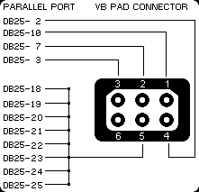
To read data from the controller by hand drive Reset (data latch) high, then the first bit from the controller will be ready to read before the first tick of the clock. From there drive the clock high and read a bit, repeat an additional 15 times, and end with the clock high. Everything is latched on the rising edge, on the data latch line or the clock. Also the bits are inverted a High value means no button was pushed. Bit1 should always be low (a logical 1) and Bit0 is the battery status bit, it should be ignored. The controller is powered from pin 2 even though pin6 is the power from the batteries. It isn't necessary to switch the controller on to get it to work.
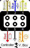
Controller Connector - looking into plug on end of cable.
An adapter can be built that allows the use of the VB's controller on a PC. Five of it's wires must be attached to the PC's parallel port. Once the adapter is made, you can use a program like SNESKey (http://www.csc.tntech.edu/~jbyork/) to read the controller, or you can read it by hand using the above info.
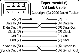
Link Port
The Link Port is a syncronous serial port. There is a 'clock' line that all transmissions are synchronized on. This clock is, by default, driven at 50KHz (20 µs period), and each data bit is sent on a rising edge. Data is transmitted/received 8 bits at a time starting with the MSB. At the default clock rate it takes 160 µs to complete a transmission. There is a generic control line that can be used to control the flow of communication. Also it appears there is a Synch In/Out pair that helps the VB to synch the send and receive data to the clock. There is a clock pull with a 20 ms period driven out of the Synch Out line at power up of the VB. The full pinout of the Link Port isn't known at this time, here is the pin out as it stands now.
 |
Cartridge
 |
| Top | ROM | RAM | ROM | RAM | Bottom |
|---|---|---|---|---|---|
| 1 | GND | GND | 2 | ||
| 3 | /WE | /WE (27) | ? | 4 | |
| 5 | ? | (/CS1) 20 | 6 | ||
| 7 | CS2 (26) | +5VDC | +5VDC | 8 | |
| 9 | /RDY | ? | ? | 10 | |
| 11 | A18 (2) | ? | 12 | ||
| 13 | A17 (3) | A20 (44) | 14 | ||
| 15 | A7 (4) | A7 (3) | A19 (43) | 16 | |
| 17 | A6 (5) | A6 (4) | A8 (42) | A8 (25) | 18 |
| 19 | A5 (6) | A5 (5) | A9 (41) | A9 (24) | 20 |
| 21 | A4 (7) | A4 (6) | A10 (40) | A10 (21) | 22 |
| 23 | A3 (8) | A3 (7) | A11 (39) | A11 (23) | 24 |
| 25 | A2 (9) | A2 (8) | A12 (38) | A12 (2) | 26 |
| 27 | A1 (10) | A1 (9) | A13 (37) | 28 | |
| 29 | A0 (11) | A0 (10) | A14 (36) | 30 | |
| 31 | /CE (12) | A15 (35) | 32 | ||
| 33 | GND | A16 (34) | 34 | ||
| 35 | /OE (14) | /OE (22) | /BYTE (33) | +5VDC | 36 |
| 37 | D0 (15) | D0 (11) | D15 (31) | 38 | |
| 39 | D8 (16) | D7 (30) | D7 (19) | 40 | |
| 41 | D1 (17) | D1 (12) | D14 (29) | 42 | |
| 43 | D9 (18) | D6 (28) | D6 (18) | 44 | |
| 45 | D2 (19) | D2 (13) | D13 (27) | 46 | |
| 47 | D10 (20) | D5 (26) | D5 (17) | 48 | |
| 49 | D3 (21) | D3 (15) | D12 (25) | 50 | |
| 51 | D11 (22) | D4 (24) | D4 (16) | 52 | |
| 53 | +5VDC | +5VDC | 54 | ||
| 55 | (Pin 55-57) | (Pin 56-58) | 56 | ||
| 57 | (Pin 55-57) | (Pin 56-58) | 58 | ||
| 59 | GND | GND | 60 | ||
1	N/C
44	N/C (A20 on 32MBit ROM)
23	+5VDC
33	/BYTE	(Held high; Chip should be in Word mode)
13, 32	GND
1	N/C
14	GND
28	+5VDC
7. CPU
Overview
The Virtual Boy is based on NEC's v810 CPU core with the following added features:
The CPU core may have additional floating point opcodes as well.
The v810 CPU is based on a 32-bit RISC (Reduced Instruction Set Computer) architecture using a combination of 16-bit and 32-bit instructions to reduce the compilation size. It has 32 general-purpose registers (r0-r31), a Program Counter (PC), and 10 system registers. All registers are 32-bits wide, and all general-purpose registers can be used in any register operation as either data and/or address register. Register 0 (r0) is the 'zero' register, its contents are always zero.
General Purpose Register Summary
| Register | Name | Description |
|---|---|---|
| r0 | ZREG | Zero register; Always holds zero |
| r1 - r25 | N/A | General purpose |
| r26 | BSDSTOFF | BitString destination bit offset |
| r27 | BSSRCOFF | BitString source bit offset |
| r28 | BSLEN | BitString length register |
| r29 | BSDSTADD | BitString destination address register |
| r30 | BSSRCADD | BitString source address register |
| r31 | LNKPTR | Stores the return address of a JAL instruction |
System Register Summary
| Num. | Name | Purpose |
|---|---|---|
| s0 | EIPC | Saves the PC and PSW during an exception/interrupt |
| s1 | EIPSW | |
| s2 | FEPC | Saves the PC and PSW during an NMI/duplex exception |
| s3 | FEPSW | |
| s4 | ECR | Upper 16-bits (FECC) holds the exception code for a NMI/duplex exception, lower 16-bits (EICC) holds the code for exception/ interrupt |
| s5 | PSW | Program Status Word; Flags indicating status of the CPU |
| s6 | PIR | Identifies the CPU type number |
| s7 | TCW | Task control word; Controls floating-point operations |
| s8-s23 | Reserved | |
| s24 | CCW | Cache control word; Controls the on-chip instruction cache |
| s25 | ATR | Address trap register; When the address in this register matches the PC value execution jumps to a predefined address. |
| s26-s31 | Reserved | |
The PSW (Program Status Word) is a set of flags that indicates the status of the CPU and the result of certain instruction executions. In particular the flags CY, OV, S, and Z are used extensively by the conditional branch instructions.
| Bit | Name | Description |
|---|---|---|
| 31...20 | RFU | Unused fixed at 0 |
| 19...16 | IntLevel | Maskable interrupt level (0-15) |
| 15 | NP | NMI pending, non maskable interrupt is being handled |
| 14 | EP | Exception pending, exception, trap or interrupt is being handled |
| 13 | RFU | Unused fixed to 0 |
| 12 | ID | Interrupt disabled, 1: disable, 0: enable |
| 11 | DP | Debug pending, 1: fatal exception is being handled, 0: not |
| 10 | SAT | Saturate flag, 1: overflow during sat arithmetic, 0: not (v830?) |
| 9...4 | RFU | Unused fixed to 0 |
| 3 | CY | Carry |
| 2 | OV | Overflow |
| 1 | S | Sign, result is negative |
| 0 | Z | Zero, result is zero |
The v810 uses a little endian addressing, that is to say the least significant byte comes first in a multi byte sequence. The standard data types include a Byte (8-bits), HWord (16-bits), and a Word (32-bits) in both signed and unsigned form. Words must be aligned on a word boundary, with the lower 2 bits masked to zero. And HWords must be aligned on a HWord boundary, with the least significant bit masked to 0. The v810 also supports BitString and 32-bit floating-point data types.
The floating-point data type conforms to the 32-bit IEEE single format.
IEEE 32-bit floating-point Format:
| 31 | 30...23 | 22...0 | ||
|---|---|---|---|---|
| S | exp (8) | mantissa (23) | ||
BitStrings are variable length strings of bits ranging from 0 (0x00000000) to 4,294,967,295 (0xFFFFFFFF) bits long. To define a BitString you must define three parameters:
When using BitString instructions load the appropriate data as defined above into the general purpose registers r26-r30 to define the source and destination strings, before calling a BitString opcode.
The v810 supports a full 32-bit addressing space (4-gigabytes). The handling of I/O is flexible, supporting both 32-bit memory mapped I/O and a full 32-bit port mapped I/O, however the VB only utilizes the memory mapped I/O. The external data buss supports both a 32-bit data mode and a 16-bit mode, but the VB only utilizes the 16-bit mode.
Instruction Summary
Located in this separate file.
Instruction Details
[Fill in later]
Interrupts/Exceptions
[need better description of NMI, Maskable Interrupt and Exception handling]
Interrupts are events that interrupt the execution of a program. Interrupts are divided into maskable interrupts and non-maskable interrupts (NMI) i.e. reset.
Exceptions are events that interrupt the execution of a program that are generated by the program execution. For example, dividing a number by zero would generate a 'Zero Division' exception.
Interrupts and exceptions are nearly identical, except for the fact that interrupts take precedence over exceptions.
The v810 handles interrupts and exceptions through an interrupt table. When an interrupt/exception is generated, the current PC and PSW registers are saved in the EIPC/EIPSW registers. When an NMI or Duplex exception is generated, the PC and PSW are stored in the FEPC/FEPSW registers. Next, the exception cause register (ECR) is filled in with the interrupt/exception number, the PSW Int Level is incremented, the PSW EP and ID bits are set to 1 and the PC is changed to point to the vector stored in the interrupt table.
In order for a maskable interrupt to occur, the NP, EP and ID bits of the PSW must be zero. Additionally, the interrupt must have an id greater than or equal to the current Interrupt Level.
Interrupt/Exception Table
| Interrupt/Exception name | Class | Code | Handled By | Restore PC |
|---|---|---|---|---|
| Reset NMI Duplexed Exception Address trap Trap instruction (0x1n) Trap instruction (0x0n) Invalid OpCode Divide by Zero FIV (float invalid op) FDZ (float zero divide) FOV (float overflow) FUD (float underflow) FPR (float degradation) FRO (float reserved op) INT level n (n = 0 to 15) |
Interrupt Interrupt Exception Exception Exception Exception Exception Exception Exception Exception Exception Exception Exception Exception Interrupt |
N/A 0xFFF0 0xFFD0 0xFFC0 0xFFBn 0xFFAn 0xFF90 0xFF80 0xFF70 0xFF68 0xFF64 0xFF62 0xFF61 0xFF60 0xFEn0 |
0xFFFFFFF0 0xFFFFFFD0 0xFFFFFFD0 0xFFFFFFC0 0xFFFFFFB0 0xFFFFFFA0 0xFFFFFF90 0xFFFFFF80 0xFFFFFF60 0xFFFFFF60 0xFFFFFF60 0xFFFFFF60 0xFFFFFF60 0xFFFFFF60 0xFFFFFEn0 |
undefined next PC current PC current PC next PC next PC current PC current PC current PC current PC current PC current PC current PC current PC next PC |
The v810 isn't set up to handle more than one interrupt at a time, but it can handle up to 2 exceptions. In order to support multiple interrupts at a time, your interrupt handling code must: [verify]
[describe returning from an interrupt/exception]
Reset/Misc.
Power on reset causes the system registers to initialize to the following:
| Register | Description | State |
|---|---|---|
| PC | Program Counter | 0xFFFFFFF0 |
| EIPC | Status saving register for interrupt | Undefined |
| EIPSW | ||
| FEPC | Status saving register for NMI | Undefined |
| FEPSW | ||
| FECC | Interrupt cause register | 0x0000 |
| EICC | 0xFFF0 | |
| PSW | Program status word | 0x00008000 |
| r0 | Zero Register | Fixed to 0x00000000 |
| r1 to r31 | Gen. Purp. Reg. | Undefined |
After initialization, program execution jumps to the reset vector at 0xFFFFFFF0 and begins execution.
